Blog
Advantages of AFM-on-a-chip
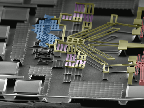
One of the most striking features of the nGauge AFM chip is its minuscule size. All of the electromechanical components that are required for an AFM to obtain an image have been integrated onto a single chip with a volume of about 0.25 mm3, which is several orders of magnitude smaller than the scanners and sensors in conventional systems. This article explains the great benefits that were achieved through our efforts to aggressively miniaturize an AFM instrument.
The Physics of Scaling
It has long been known that scaling a scanning probe microscope (SPM) could improve its performance drastically. In fact, soon after the co-creation of the first AFM prototype by Gerber, Quate and Binnig, students in Cal Quate’s lab at Stanford demonstrated a micromachined Scanning Tunneling Microscope (STM) that achieved atomic resolution. The potential for smaller SPMs to achieve superior vibration immunity, higher scan speeds, lower costs through batch fabrication, and array operation were apparent as early as the 1990’s, but the first product is only now being commercialized by ICSPI. Some of the benefits of miniaturization are discussed in this post:
- Vibration Immunity
- Drift
- Precision Scanning
- Dense Integration
- Speed
- Place the AFM directly on the sample
- Array Operation
Vibration Immunity
We are surrounded by vibrations of all kinds that span a wide range of frequencies. Building vibrations may come from elevators, doors, HVAC systems, people walking around, being on an upper floor of a building, a train moving by, among many other sources. These inescapable vibrations can range from frequencies of below 1 Hz up to about 1 kHz. Other vibration sources may come into play at higher frequencies, like sound waves and mechanical systems.
All mechanical systems have frequencies at which they sensitive – known as resonant frequencies. Vibrations can couple into the resonant modes of the system. Vibrations negatively affect AFM scans by introducing noise into the images.
A large, heavy AFM has low frequency resonant modes that are more susceptible to low-frequency building vibrations. The conventional approach to suppressing vibrations has been to isolate the AFM by placing it in an acoustically shielded box on a heavy granite slab that may be suspended with springs. This adds cost, makes the instrument larger and heavier, and limits where the system can be placed.
At ICSPI, we recognized that the best way to solve this problem was to make sure that the resonances of the AFM were much higher than building vibrations. High frequency resonant modes are less susceptible to building vibrations. To do this, we made the nGauge AFM much smaller than conventional AFMs.
This is an example of the importance of scaling laws. If we shrink an object’s dimensions down by a factor of 100x, its mass shrinks down by a factor of 1,000,000x! The resonant frequency of a spring-mass-damper system is inversely proportional to the square-root of its mass, so in this case, miniaturization has a profound impact.
The nGauge system naturally rejects building vibrations due to its low mass and high resonant frequency. That’s why the nGauge is portable and can image on almost any standard surface – without vibration isolation.
Drift
Have you ever found an interesting feature on a sample and tuned your AFM to achieve the highest image quality, only to watch helplessly as it drifts out of your field of view? Drifts may be caused by changes in ambient temperature, expanding and contracting the mechanical path between the tip and sample. The resulting instabilities are exacerbated by the non-ideal properties of piezoelectric scanners. The conventional solution to this problem has been to throw money at it. Temperature-controlled chambers, position sensors in a closed-loop configuration, and the use of materials with low thermal expansion coefficients are some examples of expensive solutions.
Scaling laws are relevant here, too. By shrinking down the entire instrument, any thermal drifts will be suppressed linearly with the scaling factor. It is critical to keep the mechanical path from the tip to the sample as short as possible. This video demonstrates the nGauge instrument imaging the same region of a sample over the course of a weekend.
Precision Scanning
Conventional AFMs are built in a machine shop with precision that comes at a high price; their scanners are based on piezoelectric materials that require expensive high-voltage electronics to drive and possess well-known non-ideal material properties that give rise to creep and hysteresis problems.
When we design our AFM chips, our features are placed on a 25 nanometer grid. The precision we achieve across our design is about 1000x better than anything that comes out of a machine shop; we use the same lithography and etching techniques that were developed by the semiconductor industry to manufacture transistors, which are some of the smallest, most ubiquitous, and least expensive products on earth. We believe that the precision and cost benefits of our CMOS-MEMS approach will have a profound impact on the use of AFMs in industry.
Dense Integration
A single-chip AFM comprises electromechanical lateral and vertical actuators, a thermal-piezoresistive resonator, differentially balanced temperature and force sensors, a motion-amplifying flexural suspension, and a sharp tip. The fact that the actuators and sensors are collocated in the same beam improves the robustness of the control of tip-sample interaction forces. A CMOS-MEMS AFM’s actuator is located within the cantilever, which simplifies the dynamics of the resonant system. Electronics may also be integrated in the CMOS chip in order to improve the signal-to-noise ratio (SNR) of the instrument. This capability will enable significant improvements in resolution and stability.
Speed
One of the biggest disparities between AFMs and other types of microscopes is their scanning speed. Large masses must move slowly to avoid resonances that are deleterious to image resolution, so smaller scanners are desirable. There have been several research demonstrations of video-rate AFM, but none are commercially available or practical for everyday use. The nGauge system experiences improvements in speed with every design iteration, and the backwards-compatibility of our chips means that the instrument improves consistently, while conventional AFMs approach obsolescence from the day they are purchased.
Array Operation
Our long-term vision at ICSPI is to create vast arrays of AFMs at the wafer level. The microfabrication processes that we use to manufacture our AFMs are well-established and routinely applied to leverage economies of scale by the CMOS industry. These arrays will enable rapid nanoscale metrology over large areas to enable unprecedented manufacturing precision. The CMOS-MEMS manufacturing approach is uniquely capable of realizing large arrays with integrated electronics to perform simultaneous imaging over practical surface areas. Stay tuned for a blog entry on our first AFM arrays, which are under development right now!
Conclusion
The nGauge system represents the culmination of a decade of research to design an AFM from the bottom up, with the physics of scaling in mind. The benefits of microfabrication in a CMOS process include improved vibration immunity, suppression of drifts, precision scanning, dense integration, higher scan speeds, freedom from sample volume constraints, and array operation.

Book a Demo
Get in touch with us today to book a demo and see the future of AFM technology.