Can AFM measure in 3D?
Can atomic force microscopy measure in 3D?
The short answer is: yes! Atomic force microscopy (AFM) is a three-dimensional (3D) imaging technique. AFM collects topography data (in the Z direction) while scanning laterally (in X and Y). However, AFM is a surface technique, meaning that AFM can collect 3D data of the surface of a sample but it cannot collect 3D data inside of a sample. We’ll discuss techniques that can collect 3D data inside of a sample later in the post.
In this post you’ll learn:
- How does AFM collect 3D data?
- Why is 3D data useful?
- What does the 3D data of AFM look like?
- What is “3D AFM”?
- What techniques can I use to collect 3D data inside a sample?
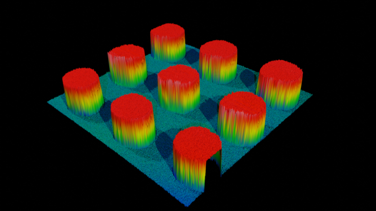
AFM doesn’t just tell you if a surface is smooth or rough; it quantifies the roughness down to the nanoscale level. Researchers, engineers, and scientists rely on AFM to characterize surfaces for applications ranging from microelectronics to biotechnology. The reason is that AFM provides high-fidelity, high-resolution 3D data on virtually any solid surface.
How does AFM collect 3D data?
AFM collects three-dimensional (3D) data by scanning a sharp probe over the surface of a sample and measuring the interaction forces between the probe and the sample. The AFM probe, typically a sharp tip attached to a cantilever, is brought into close proximity or into contact with the sample surface.
Animation of an AFM scan of sintered aluminum oxide from 2D grayscale to 3D topography image. Collected with the Redux AFM.
The AFM probe is positioned above the sample, and the feedback loop is used to control the distance between the probe and the sample. The probe is then raster-scanned across the surface of the sample in the x and y directions. During this process, the topography of the sample is recorded at each point at the nanoscale.
Why is 3D data useful?
There are many applications where nanoscale 3D data is useful. A major use case for AFM is in semiconductor manufacturing and microfabrication, where the thickness of the film must be measured with sub-nanometer precision because even 0.5 nm off the target is the difference between a product passing or failing quality control!
Because 3D data is quantitative, it can provide information like the roughness of a surface. The surface roughness is important, for example because it can dictate whether a surface reflects light or not, depending on the level of polish. Using AFM can help refine a polishing protocol to make sure products are being polished to specification. For medical applications, if a surface is too rough or too smooth, it may not work. (For more information on AFM for surface roughness, check out our blog post Can AFM measure surface roughness?)
Structure-property relationships can also be developed from 3D data. Sometimes these relationships are surprising. For example, the roughness of a film can dictate whether the film will work as an adhesive or not.
Keep in mind that although often used for measuring at the nanoscale, AFM can also be used for measurements at the microscale.
There are many applications for AFM, because virtually any solid sample can be measured, and the data is 3D and quantitative. AFM data goes far beyond just topography or morphology data: AFM allows you to collect roughness, step heights, particle size and distribution, as well as spatial distribution of components with different materials with phase imaging. Check out our application page to see more applications of AFM.
Can optical microscopes and SEM collect 3D surface data?
Optical microscopy and scanning electron microscopy are typically 2D techniques and they cannot collect 3D data in the same way as AFM. The reason is that in an AFM image, each pixel represents height data, so it contains quantitative information at very high resolution. The image from an optical microscope or SEM is still two-dimensional data.
However, there are a few adjacent techniques that can collect 3D data, but with lower resolution than AFM.
One optical technique that can be used to collect 3D surface data is confocal microscopy, which uses a pinhole and laser illumination to selectively collect light from a specific focal plane while rejecting out-of-focus light. By scanning through different focal planes, you can create a series of 2D optical sections, which can be stacked to generate a 3D image. The vertical resolution of a confocal microscope is about 500 nm, whereas in AFM is several orders of magnitude higher, at <0.5 nm. The lateral resolution of a confocal is limited by the wavelength of light so it is constrained to about 200 nm, whereas AFM lateral resolution can be single-digit nm (depending on the probe radius).
Another optical technique for 3D surface data is interferometry. A popular type is white-light interferometry (WLI). As its name suggests, WLI uses the interference of white light to collect 3D data of a surface. Like other optical techniques, the lateral resolution is limited by the wavelength of light, to about ~160 nm. The vertical resolution can be 1 nm or better. However, WLI is not ideal for measuring around steep cut-offs, especially where there are multiple steep cut-offs in the same area, like gratings.
What is "3D AFM"?
Somewhat confusingly, there is also a term called “3D AFM”. This is an advanced technique for gathering quantitative “topography” data in all three dimensions. Typical AFM gathers topography data in the Z axis only as the cantilever moves in the Z axis, while it moves in the X and Y axes. In 3D AFM, the tip moves in the X and Y axes while also moving the Z axis, so it can collect measurements of the sidewalls of a feature. 3D AFM is most commonly used in semiconductor manufacturing and microfabrication, where sidewall roughness can be important.
What techniques can I use to collect 3D data inside a sample?
The go-to technique for collecting 3D data inside a sample is computed tomography (CT). CT is an X-ray technique, where the sample is placed between an X-ray source and a detector array. The sample is rotated 360 degrees and as it is rotated, the X-ray images are acquired at multiple angles. The 2D images are then reconstructed to form a 3D image of the inside of the sample.
Summary
In summary, AFM is a powerful technique that can collect quantitative 3D data of the surface of a sample with extremely high lateral and vertical resolution. AFM data goes beyond traditional optical microscopes and SEM to provide true 3D surface data. Certain optical techniques can be used to collect 3D surface data as well, but with poorer resolution. There are many applications where 3D topography data is useful. For more information on applications of AFM, check out our applications page.

Interested in learning more about AFM?
Speak with an application engineer today to see how AFM can help with your research and process development.