AFM for Nanoimprint Lithography
Common uses of AFM for NIL
Nanoimprint Lithography (NIL) is a templating method for generating micro- and nanostructures on various materials with applications in the semiconductor industry, display, biology/life science and more. NIL involves pressing a resist beneath a patterned master template at the nanoscale to transfer the pattern onto the resist. Techniques like Thermal, UV-cured, and nano-contact imprint lithography are commonly employed, each with distinct tradeoffs.
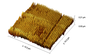
Atomic Force Microscopy (AFM) is useful cor collecting high-resolution 3D imaging essential for measuring critical dimensions (CDs), surface roughness, and detecting defects of NIL molds and fabricated structures.
Benefits of AFM for NIL
A major benefit of AFM over techniques like scanning electron microscopy (SEM), is that AFM can scan virtually any solid sample, including non-conductive and transparent samples. AFM is a non-destructive technique that requires minimal sample preparation: patterned samples can be readily scanned.
Quality control in NIL relies heavily on maintaining CD and mitigating local defects. CD encompasses the size, pitch, and other specifications of the imprinted pattern, while local defects range from contamination to non-uniformity in transferred patterns.
AFM plays a vital role in characterizing NIL products, offering sub-nanometer resolution in the Z-axis and nanometer resolution in the XY axes. It enables precise comparison between master templates and imprinted samples, facilitating assessment of pattern transfer quality and defect presence.
AFM’s versatility make it an excellent choice for NIL applications alongside complementary techniques like optical microscopy, SEM, and ellipsometry. AFM excels in providing reliable CD measurements, precise Z-axis data, and detailed local defect characterization, crucial for ensuring the integrity of NIL processes.
Want to read more?
Download our 5-page application note that covers multiple samples fabricated using NIL, the types of defects AFM was able to detect, and a comparison between AFM, SEM, and other techniques for NIL.
Speak with an expert
Interested to learn more about how AFM can help you with your nanoimprint lithography processes?