Atomic Force Microscopy (AFM) is a long-standing and versatile tool for inspecting a wide array of microfabricated devices, such as microfluidics, semiconductors, displays, metasurfaces and other microfabricated optics. In contrast to scanning electron microscopy (SEM), which offers only two-dimensional images lacking quantitative height data, AFMs can quickly collect detailed three-dimensional images, providing precise measurements of feature height, critical dimension, and roughness.
Operating under ambient conditions without the need for complex sample preparation, AFM is particularly convenient for imaging non-conductive samples, saving both time and eliminating the need to coat (and destroy) non-conductive samples. Finally, AFM is ideal for measuring trench depths where destructive FIB-SEM may have to be used.
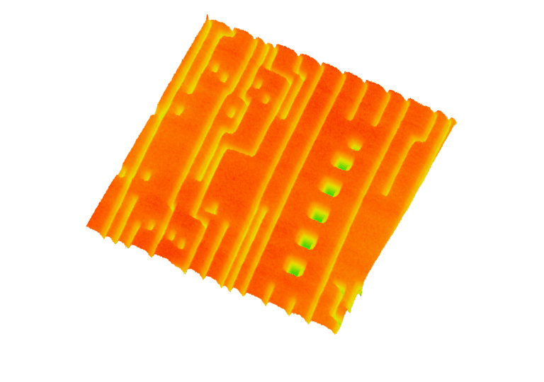
Illustrated through the inspection of the photoresist patterned on a coupon, AFM excels at accurately measuring feature height and dimensions with high precision, revealing deviations from expected shapes and dimensions. Unlike SEM, AFM provides precise measurements of each feature, enabling tighter control over microfabrication processes.
3D representation of the critical dimensions of the photoresist on a patterned wafer. Coupon from a 300-mm wafer manufactured with 193i lithography.
AFM for surface roughness
AFM is also ideal for highly accurate surface roughness measurements and statistical analysis crucial for various semiconductor applications, such as verifying wafer roughness of bare wafers (e.g., for specialty III-V wafers), post-chemical mechanical polish (CMP), or the roughness of films grown on a substrate. Compared to typical stylus profilometers, the lateral resolution of AFM is usually at least 100x more precise, because of the sharpness of the tip, enabling the highest accuracy for surface roughness.
ICSPI's AFMs for microfabrication
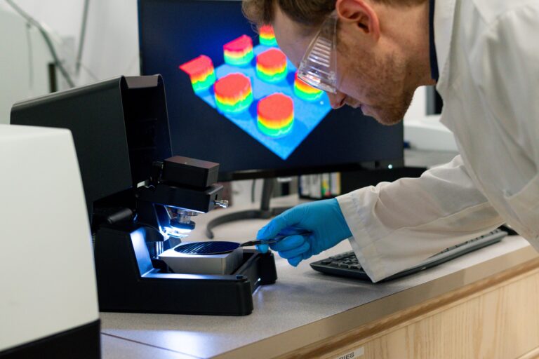
ICSPI’s nGauge and Redux AFMs are ideal for characterizing microfabricated structures, whether they are on a coupon, wafer or other substrate. In particular, the Redux AFM can accommodate wafers up to 100 mm in size and it is equipped with a motorized XY stage, so users can quickly and precisely navigate to a region of interest on the sample.
Loading a 100-mm patterned wafer onto the Redux Atomic Force Microscope.
Speak with an expert
Interested to learn more about how AFM can help you with your microfabrication processes?