AFM for Ceramics
Common uses of AFM for ceramics
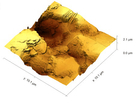
Atomic Force Microscopy (AFM) opens up options for characterization of ceramics at the micro and nanoscale, offering detailed three-dimensional images that provide insights into surface roughness, grain size, and morphology. These properties are vital for applications across various fields such as electrical insulation, silicon wafer handling, sensor chip carriers, electronic device packaging, and heat management in laser and electronic systems.
A major benefit of AFM is that it can scan virtually any solid sample, including non-conductive and transparent samples. In addition, AFM can scan these samples non-destructively.
A common application involving ceramics is sintering and serves as an excellent case study of the usefulness of AFM. Sintering, a common manufacturing technique for ceramics, involves fusing ceramic grains under heat to form a solid part without reaching the material’s melting point, enhancing the density and decreasing porosity. Commonly used materials for sintering include aluminum nitride (AlN) which possesses qualities of low electrical conductivity alongside high thermal conductivity making it useful for heat sink applications. Ceramic sintering’s complexity, influenced by variables like pressure and temperature, directly affects the grain size and surface morphology of the product.
ICSPI's AFMs for characterizing ceramics
Our AFM instruments, the nGauge and Redux AFMs, can quickly and accurately characterize ceramic materials. Our AFMs’ ability to collect high-resolution three-dimensional data facilitates the development of structure-property relationships, essential for process control and optimization in ceramic manufacturing.
Speak with an expert
Interested to learn more about how AFM can help you with your ceramics-based processes?