Measuring E-Beam Lithography Resolution with Atomic Force Microscope
Measuring the Resolution of E-Beam Lithography Patterns with Atomic Force Microscopy
The Breaking Taps garage lab has a new tool: a scanning electron microscope! SEMs can also be used for electron-beam lithography (also known as e-beam lithography or EBL). In this video, the host of Breaking Taps, Zach Tong, shows his results of using his tabletop SEM for patterning micro- and nanoscale patterns. An nGauge atomic force microscope (AFM) unit is used to do the high-resolution characterization of the patterns (measuring line widths, heights and inspecting contamination) and was crucial in troubleshooting the process development.
E-Beam lithography background
The concept of e-beam lithography shares similarities with photolithography in terms of exposing a resist material and developing it to form positive or negative patterns. However, the key difference lies in the use of electrons as the primary energy source. This distinction brings about several advantages and challenges associated with e-beam lithography.
One notable advantage of EBL is its incredible resolution capabilities. The resolution of a lithographic process is determined by the wavelength of the energy source. Electrons have an extremely small wavelength, ranging from two to ten picometers. This smaller wavelength allows EBL to achieve unparalleled levels of precision that are difficult to match with photons.
However, one major downside of EBL is its direct-write nature: EBL involves rastering a beam of electrons across the resist material to form the desired pattern. Consequently, EBL is primarily utilized in research institutions and labs where throughput is less important than achieving fine resolution.
Comparing optical, SEM and AFM for measurement resolution
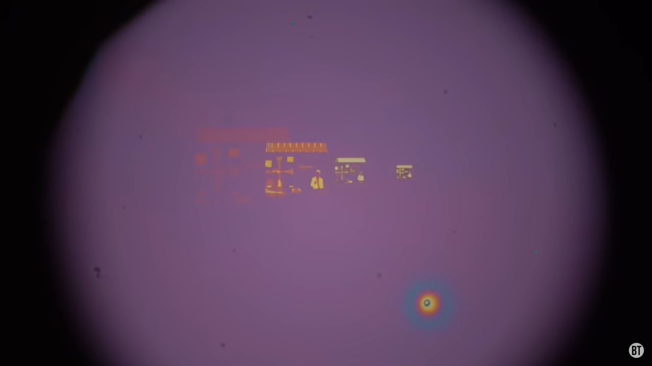
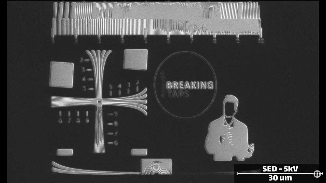
The SEM patterns the features on PMMA, which was previously coated onto a doped silicon wafer. Once the patterns are developed, it’s time to take a look! The host first looks at the patterns using an optical microscope (at 10:45). As the patterns get smaller and smaller, it’s impossible to use the optical microscope because it doesn’t have sufficient resolution. Then he moves to SEM (at 12:38), which does not work particularly well because the resist is a polymer and builds up charge. There also isn’t a lot of contrast between the resist and the wafer underneath, so it’s difficult to get a good image.
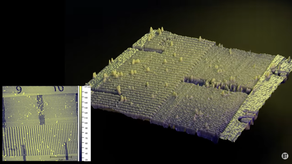
To really measure the patterns, Zach uses an nGauge AFM (at 13:07). AFM is able to measure the sizes of the features, such as the height and line width, with sub-nanometer precision. Particles and contamination are also very clearly identified.
How AFM is used for characterizing EBL patterns
AFM aids in identifying and addressing potential issues, such as particles or contamination present in the patterns. By examining the samples under AFM, researchers can differentiate between dust and residual resist, facilitating the debugging process. Additionally, the video highlights the dose dependence of the EBL process. The host explains how exposing different regions to varying electron doses results in controlled etching depths. AFM complements this by verifying the progress of developing the resist through height measurements. The AFM measurements confirm the reliability and consistency of the EBL process.

Interested in learning more about AFM?
Speak with an application engineer today to see how AFM can help with your research and process development.